Hardware
Hardware Implementation of the Tagma Primitive
Abstract
Tagma1 is a 16-bit coordinate primitive: a fixed Unicode block (U+AC00–U+D7A3) with a closed-form composition formula, three independent axes, and zero collision probability. The primitive is substrate-independent. Its definition is one formula, and its realizations differ only in the material that evaluates it. The software realization is the reference implementation in Rust and C++ 2 3; the hardware realization is the subject of this whitepaper series: a combinational decoder with its inverse (the compose unit) and the field-wise distance unit, a gate-level synthesis flow, an FPGA demo on the Upduino 3.1, and a chton SRAM segment store modeled behaviorally pending the macro.
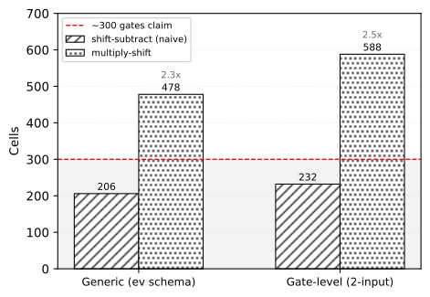
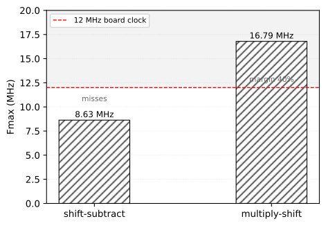
Everything in this series is measured, not claimed. The decoder is verified exhaustively over all 11,172 valid syllables in three independent channels (formula, Rust reference, gate netlist), and formal equivalence proves the RTL and the synthesized netlist identical over all 2^16 inputs. The measured gate count is 478 cells in the ev-compatible generic schema and 588 cells in a 2-input gate-level estimate, with 201 LUT4 plus 41 carry cells on iCE40. The demo closes the 12 MHz board clock at 16.79 MHz Fmax (59.55 ns critical path after place and route).
Two findings frame the series. First, the ~300 gate claim of the Tagma whitepaper holds for the naive shift-subtract decoder (206 to 232 cells), but timing closure on a 12 MHz board requires a multiply-shift structure that costs roughly 2.5x more gates. Second, the hardware is not a speedup for the N=1 dense case: the entire 11,172-entry space fits in L1 cache, which the software already exploits at 0.38 ns per access. The hardware value is energy, determinism, and physical embedding, not per-operation speed.
1 Scope and relation to the primitive
The hardware track does not redefine Tagma. The composition formula, the axis ranges, and the 11,172-entry space are identical to the software definition:
\[C(i,m,f) = \text{U+AC00} + 588i + 28m + f, \quad 0 \leq i < 19,\; 0 \leq m < 21,\; 0 \leq f < 28\]
What changes is the substrate. The software realization evaluates the formula with arithmetic in Rust; the hardware realization evaluates it with logic gates. The two must agree on every input, and the verification pipeline in this series enforces exactly that. The layer map is shown in Figure Figure 1.

One boundary correction is part of this work: the last valid syllable is U+D7A3, not U+D7AF. The block contains exactly 11,172 syllables and U+AC00 + 11,171 = U+D7A3. Inputs in U+D7A4..U+D7AF decode to an out-of-range initial axis and are structurally invalid; the tagma_core reference documents these as filler positions.
2 Realization status
The claim of this series is bounded by what is realized. The three operations of the primitive are realized as RTL and verified end to end: the decoder, the compose unit (the decoder’s inverse), and the distance unit. The gate-level netlist simulation and the formal-equivalence check cover all three.
Two items are documented but not yet realized. The segment store is a behavioral model of the address map, pending the OpenRAM macro that needs a PDK install. The physical FPGA demonstration is pending a board, though the bitstream and the timing report are generated. Where a result depends on an unrealized item, the document states the dependency in place.
3 Measured results summary
The numbers below are the authoritative hardware figures for the Tagma primitive. They replace the approximate “300 gates in 28nm” phrasing in earlier software documents with measured values from the open toolchain (Yosys, nextpnr, icetime). The gate trade-off is shown in Figure Figure 2 and the clock closure in Figure Figure 3.
| Metric | shift-subtract (naive) | multiply-shift (current) |
|---|---|---|
| Generic cells (ev schema) | 206 | 478 |
| Gate-level estimate (2-input) | 232 | 588 |
| iCE40 LUT4 + SB_CARRY | 95 + 66 | 201 + 41 |
| PnR ICESTORM_LC (UP5K) | 177 | 255 |
| Logic levels | 72 | 33 |
| Critical path | 115.90 ns | 59.55 ns |
| Fmax | 8.63 MHz | 16.79 MHz |
| Meets 12 MHz board clock | no | yes |
The verification status across all channels:
| Check | Result |
|---|---|
| Exhaustive RTL simulation (formula mode) | PASS: all 11,172 code points |
| Golden anchors (Rust reference mode) | PASS: all 11,172 |
| Gate-level netlist simulation | PASS: all 11,172 |
| Formal equivalence RTL vs netlist | proven, 50 cells, all 2^16 inputs |
| Compose, the decoder inverse (formula + golden) | PASS: 32^3 axis combinations and 11,172 anchors |
| Distance (formula + golden) | PASS: 11,172 code points against two references and a varying-operand sweep |
| Compose and distance equivalence | proven over 2^15 axis combinations and 2^32 input pairs |
4 Verification pipeline
Every hardware artifact is checked against the Rust reference, which is the single source of truth for the primitive’s behavior. The golden exporter writes the full coordinate decomposition to a vector file; the RTL simulation and the gate-level simulation both read it; the formal equivalence check closes the loop between the RTL and the synthesized netlist. The pipeline is shown in Figure Figure 4.

The pipeline runs in CI through make -C hw check in the syntagma repository, so the numbers in this series are reproducible from a clean checkout when Verilator and Yosys are installed.
5 Documents
| Document | Description |
|---|---|
| RTL | Decode, compose, and distance: structure and the verification pipeline |
| Synthesis | Gate counts, cell mixes, and the naive vs multiply-shift trade-off |
| FPGA | Upduino 3.1 demo, place and route, timing report |
| Memory | chton SRAM segment store and the L1 cache analysis |
| Reference Implementation | Hardware reference: engineering decisions, development experience, next steps |
License
The hardware design sources documented in this series, the Verilog RTL, the synthesis and place-and-route scripts, the board and timing constraints, and the OpenRAM and OpenROAD flow, are licensed under the CERN-OHL-P v2, the permissive variant of the CERN Open Hardware Licence version 2. The full text is in hw/LICENSE in the syntagma repository. The software reference implementation under sw/ remains under the Apache License 2.0.
References
Footnotes
Tagma whitepaper: docs.ssccs.org/projects/syntagma/tagma↩︎
synTagma: a spatial coordinate space computing system based on the Tagma primitive. Docs, Repository: Github (Pre-release, Apache 2.0)↩︎
The hardware sources live in the syntagma repository under
hw/: github.com/ssccsorg/syntagma/tree/main/hw↩︎