Memory
The SRAM segment store and the L1 cache analysis

1 The segment store
The coordinate space maps onto physical memory as a flat array: 11,172 slots of 16 bits each, addressed by the 14-bit offset from the decoder. The single-port SRAM macro is configured for SkyWater 130nm, and the macro generation is pending an OpenRAM PDK install. What is verified today is a behavioral model of the same address map and read/write behavior, checked exhaustively over all 11,172 slots with the 5,212 reserved addresses reading zero. The OpenRAM configuration is:
#| eval: false
word_size = 16          # one Hangul code point per word
num_words = 11172       # full Tagma space: U+AC00..U+D7A3, 19 x 21 x 28
num_rw_ports = 1        # single read-write port
tech_name = "sky130"
The full space is about 22 KB of raw storage, or 44 to 89 KB with values, depending on the value width. 11,172 is not a power of two; if the PDK flow requires one, the fallback is 16,384 words (2^14) with 5,212 reserved entries, since the 14-bit address space covers the valid range either way.
2 Latency: the honest comparison
Three measured paths are compared below. The software numbers come from the benchmark center sw/rust/benches/bench_hw.rs; the hardware number is the post place-and-route critical path on the UP5K. The comparison is shown in Figure Figure 1.
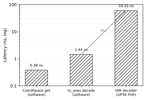
The per-operation latency comparison is the central finding of this document:
| Path | Latency | Note |
|---|---|---|
CoordSpace.get (software) |
0.38 ns | whole space in L1 cache |
Coord::to_axes (software) |
1.44 ns | reference decode |
| HW decoder (UP5K PnR) | 59.55 ns | worst-case critical path at 16.79 MHz |
For the N=1 dense case, hardware is not a speedup. The entire working set fits in L1 cache, and the software already runs at memory speed. A hardware SRAM at FPGA clock rates cannot beat that, and GHz-class SRAM would require a leading-edge ASIC whose mask cost starts in the millions of dollars. Chasing L1 speed in hardware is solving a problem the software already solved.
3 Where hardware wins
The value of the hardware realization is on other axes:
| Axis | Software | Hardware |
|---|---|---|
| Energy per access | host CPU pipeline and cache hierarchy | 22 KB SRAM at 16 MHz, orders of magnitude lower (estimate, pending power model) |
| Latency determinism | cache-dependent, variable | fixed one cycle |
| Physical embedding | impossible | the primitive becomes a device, the chton signal-layer vision |
| Streaming throughput | per-op overhead in software | one code point per clock when pipelined; wins at scale or at higher clocks |
The acceleration case appears at N greater than 1, where software falls back to sparse trees (0.87 to 53 ns per operation), and in embedded or IO paths where energy and determinism dominate over raw speed.
4 Open questions
The Sky130 standard cell flow is set up and runs in CI (hw job in the syntagma repository): ORFS on the x86 runner produces the area, timing, and power report for the registered demo top, plus the pure decoder gate count via yosys stat -liberty. The flow runs on x86 and on Apple Silicon under Rosetta; the default-on kepler-formal LEC step crashes on both and is disabled in the design config (see the syntagma devlog entry). The VCD activity trace from simulation (make sim-trace) is the input for the power estimation. The OpenRAM SRAM macro generation remains pending a PDK install.